Center for Transmission Electron Microscopy (CTEM)
With the launch of IMRI, UCI has purchased five major instruments, which include four unique TEMs and a dual-beam focused ion beam (FIB) system. IMRI is the first research lab in the Americas with the newly introduced JEOL Grand ARM and Nion Monochromated UltraSTEM HERMES200, which exceed the atomic resolution boundaries of any commercially available TEM today. All instruments have recently been installed in the new TEM facilities at IMRI. The capabilities and unique characteristics of these instruments are summarized as follows:
Nion aberration-corrected UltraSTEM 200 with a monochromated EELS system (HERMES 200)
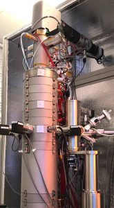
Nion HERMES 200 has the highest spatial and energy resolution of any commercially available STEM, with many critical features not found on any other instrument. The unique design of the monochromator of the HERMES system provides an energy resolution for electron energy loss spectra (EELS) of 5.7 meV when operated at 60 kV and 4.2 meV when operated at 30 kV, with a long-term energy stability of the order of 10 meV/min. This allows vibrational spectroscopy to be carried out in combination with the spatial resolution and flexibility of the TEM. Thus, this unique microscope can explore physical phenomena such as lattice vibrational modes (phonon) and chemical-bond vibrations that are spatially highly localized. Besides the monochromator, HERMES also includes an advanced aberration corrector unavailable on any other instrument, which allows individual control of all aberrations up to fifth order, providing the unprecedented STEM spatial resolution of <0.5 Å when operated at 200 kV. The Nion HERMES enables researchers to explore the atomic structure, chemical bonding, and local electronic structure of materials with the highest spatial and energy resolution in combination with ultrahigh energy resolution for EELS. It is equipped with high angle annular dark field (HAADF), medium angle annular dark field (MAADF), annular bright field (ABF), and wide/small angle bright field (BF) detectors and an advanced electron energy-loss spectrometer. The Nion UltraSTEM is the only electron microscope that operates in ultrahigh vacuum conditions (<10-10 Torr). Thus, electron beam induced contamination is avoided and samples such as graphene and other 2D materials are largely stable when imaged and analyzed at an energy less than their knock-on displacement threshold.

JEOL double spherical aberration-corrected JEM-ARM300CF “Grand ARM”
JEM-ARM300F Grand ARM TEMThe Grand ARM is the newly introduced JEOL 60-300 kV TEM, which offers a 63 pm resolution at 300 kV
for atom-by-atom characterization and chemical mapping. It features JEOL-proprietary spherical aberration correctors integrated into the image-forming system and illumination system, and an ultra-stable cold-cathode field emission electron gun. The cold field emission gun provides a high probe current in a very small probe with an energy resolution of 0.35 eV, which is ideal for the structural and chemical analysis of nanostructured materials, defects, and devices with atomic resolution. The wide pole piece gap (>6 mm) of the JEM-ARM300FC makes it possible to develop customized holders for a variety of in-situ TEM experiments to study the structure, properties, and dynamic behavior of nanostructured materials under applied fields, stress, and reactive environments. The Grand ARM uses a unique hybrid high-angle annular dark-field (HAADF) STEM detector. This detector provides a sensitivity higher than any scintillator over the entire accelerating voltage range, from 300 kV to 60 kV or less. Higher sensitivity means a better signal to noise ratio, which is important for imaging under low beam current for beam-sensitive samples such as soft and 2D materials. This microscope is equipped with a dedicated annular bright-field (ABF) detector, which makes ABF imaging easy, by just inserting the detector. There is no need to change camera lengths to adjust what is being collected on the standard bright field (BF) detector. This allows one to acquire HAADF, ABF, and BF images simultaneously over a range of camera lengths. This capability is critical for the atomic-scale structure and property analysis of materials containing both light and heavy elements. Alignment of the imaging and probe-forming correctors uses a special, easy-to-use algorithm (no standard sample is needed). The Grand ARM is integrated with a new generation direct electron detection system (the Gatan K2 IS) and the newly released OneView cameras for optimum CCD imaging. The K2 IS is the most powerful camera available for TEM imaging, a game-changer for electron microscopy, that enables the study of atomic-scale details of structural changes dynamically within TEM (up to 1600 fps). This microscope is also equipped with an electron biprism for holography, double 100 mm2 X-ray detectors for energy-dispersive spectroscopy (EDS), and Gatan 965 GIF Quantum ER imaging filter with dual-energy range EELS (DualEELS), suitable for the rapid mapping of elements with atomic resolution.
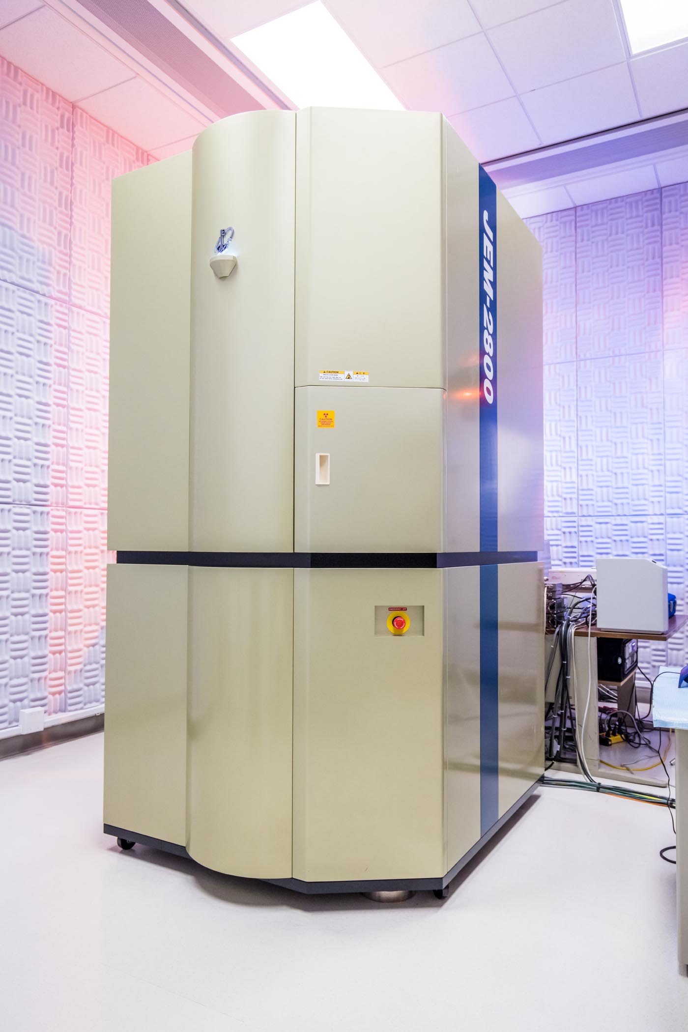
JEOL JEM-2100F Cryo-TEM
This 80-200 kV TEM is equipped with a field emission gun, a cryo stage, and a Gatan CCD camera (OneView) and a K2 Summit camera for the study of biological specimen at room and liquid nitrogen temperatures. The cryo TEM is suitable for the observation of frozen-hydrated specimens such as single proteins or two-dimensional crystals of membrane proteins. This microscope is equipped with a differential vacuum system utilizing sputter ion and diffusion pumps, eucentric motorized 5 axes side-entry goniometer with a cryo pole piece that provides a point-to-point resolution of 0.27Å with specimen tilting up to ±60°. A double-tilt cryo-transfer system (Gatan 915) allows frozen sections or suspensions to be loaded into the holder and transferred frost-free at a temperature lower than -170°C. This system includes a double tilt, liquid nitrogen-cooled specimen holder, and tools for the frost-free transfer of up to four grids. There is also a second double-tilt liquid nitrogen cryo holder with a beryllium cradle (Gatan 626) for a range of frozen samples. One can utilize the cryogenic and atomic level structural analysis capabilities of the cryo TEM to examine biological materials, large molecules, and medical biopsy samples.
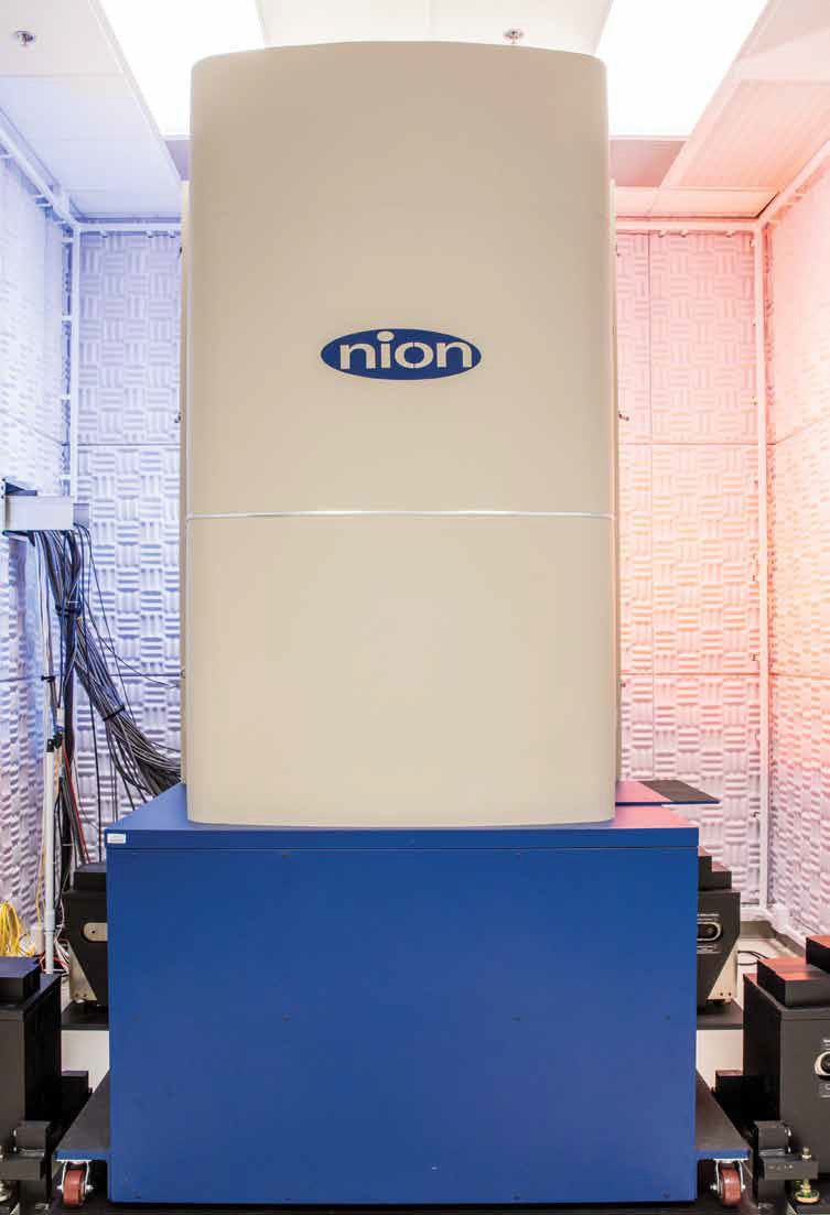
JEOL JEM-2800 S/TEM
This versatile 100-200 kV Schottky field emission TEM will serve as a workhorse for structural/chemical analysis of materials. It features high-resolution imaging in TEM, STEM, HAADF, ABF, and secondary electron (SE) modes (analytical high-resolution pole piece), ultrasensitive elemental mapping with large angle EDS (dual dry solid-state 100mm2detectors), and the Gatan OneView IS camera for imaging and in-situ observations at 320 fps. The JEM-2800 has fully automatic functions including adjustment of focus, astigmatism, contrast, brightness, crystal zone axis alignment, and specimen height. Switching between analysis modes is seamless, and quick data collection shortens turnaround time between samples. An operator navigation system and on-screen operating guide make the JEM-2800 a high throughput, user-friendly TEM for any skill level.
TESCAN GAIA-3 XMH integrated focused ion beam-FESEM
The GAIA-3 XMH FIB-SEM is TESCAN’s newest, highest-end flagship dualbeam instrument. It has a unique three-lens electron optical design capable of dedicated modes for extreme high-resolution imaging (magnetic immersion mode), enhanced depth of focus, undistorted ultra-low magnification imaging, and live 3D stereo imaging. These unique features will provide ease of use to the multi-user environment, especially for our students and young researchers. The instrument is fully equipped with beam deceleration, in-beam SE and BE detectors, retractable
TESCAN GAIA-3 GMH integrated focused ion beam-FESEM
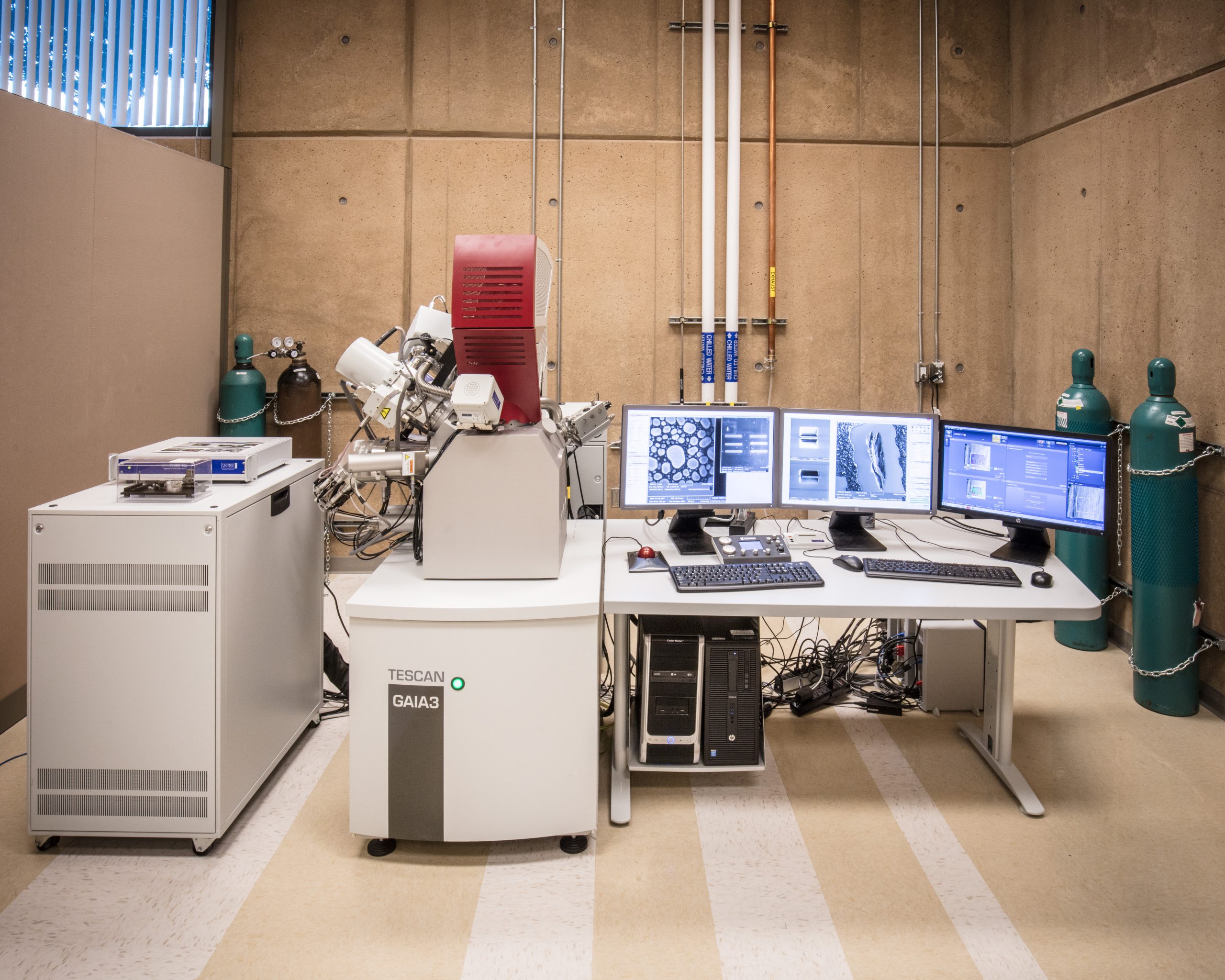
STEM and YAG BE detectors, off-axis Everhart-Thornley SE detector, SITD secondary ion detector, 5-reservoir gas injection system (W, Pt, SiOx, H2O, XeF2), in-situ plasma cleaner, electron beam lithography package, autoslicer, 3D Tomography Advanced package, electron beam induced current (EBIC) system, Oxford AZtecEnergy Advanced EDS Microanalysis System with the latest X-Max 150 mm2silicon drift detector, Oxford AZtecHKL Advanced NordlysMax2 integrated EBSD System, and Omniprobe 400 port-mounted piezo nanomanipulator, the last of which provides an ideal tool for the preparation of TEM specimens for structural imaging and chemical analysis with atomic resolution in combination with the state-of-the-art TEMs described above. The smart chamber design of the GAIA XMH FIB-SEM instrument allows for the simultaneous milling and collection of EBSD patterns without the need to move the sample. This flexibility is unique to TESCAN and will provide best-in-class accuracy and throughput for EBSD and EDS.The 3D-EDS and EBSD reconstructions are critical for understanding the structure and chemistry of materials. This FIB-SEM is the only such system that can be integrated with a time of flight secondary ion mass spectrometer (TOF-SIMS), which is planned for the future.